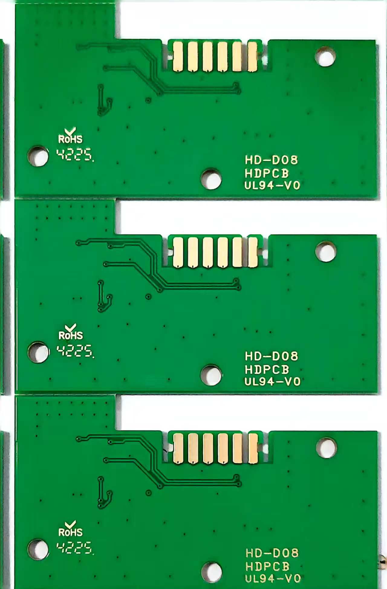
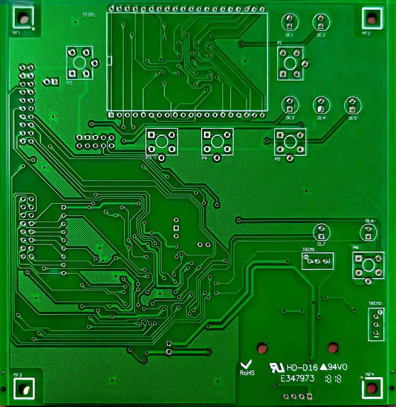
什么是双面板?
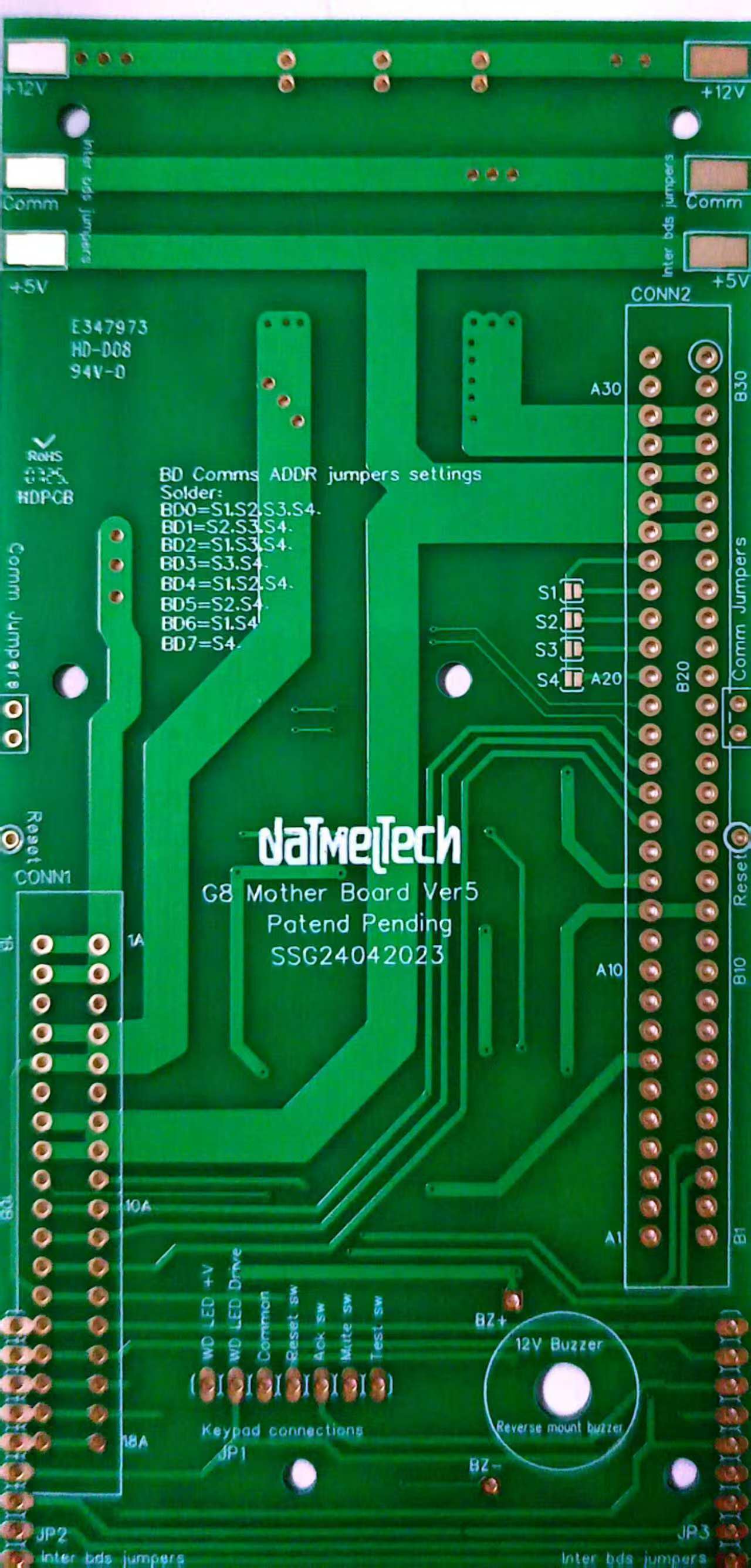
双面板是在基材两侧同时覆铜并形成线路,通过过孔实现上下层电气连接的 PCB。
双面板的特点
高线路密度
双面布线设计,线路密度显著提升,比单面板更适合复杂电路设计。
设计灵活性
上下两层均可布线,设计空间更大,布线路径选择更多,优化电路性能。
中等复杂度适用
完美平衡单面板和多层板的优势,适用于中等复杂度的各类电子产品。
性价比最优
在性能提升与成本控制之间取得最佳平衡,是多数应用的理想选择。
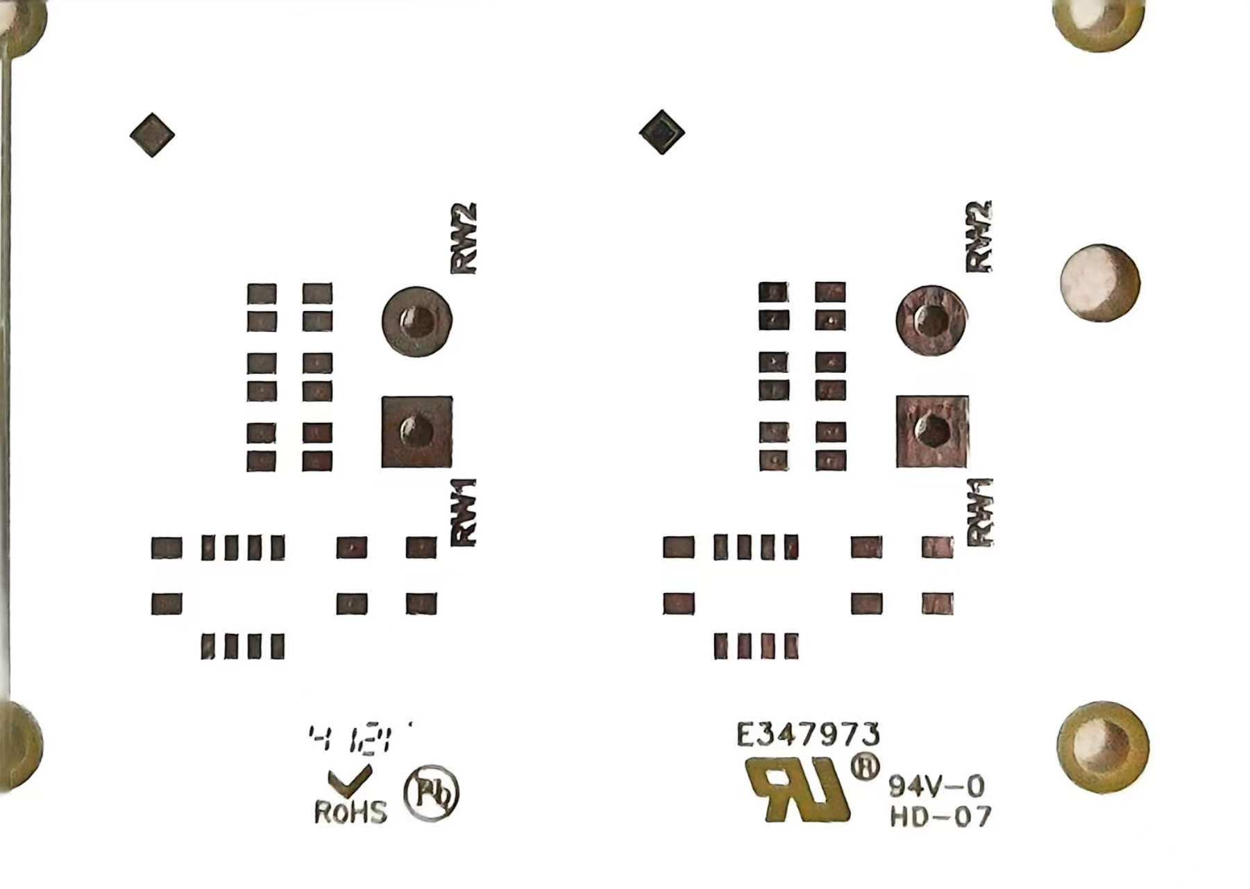
双面板主要材料
建滔 KB
生益 SHENGYI
联茂 ITEQ
南亚 NANYA
腾辉 VENTEC
国纪 ILM / GDM
金宝 JINBAO
性能等级
TG130°C
FR-4 标准等级
TG150°C
FR-4 中温等级
TG170°C
FR-4 高温等级
CTI等级
0-4级可选
✓ 以上双面板材料均已完成 UL 全系列认证。
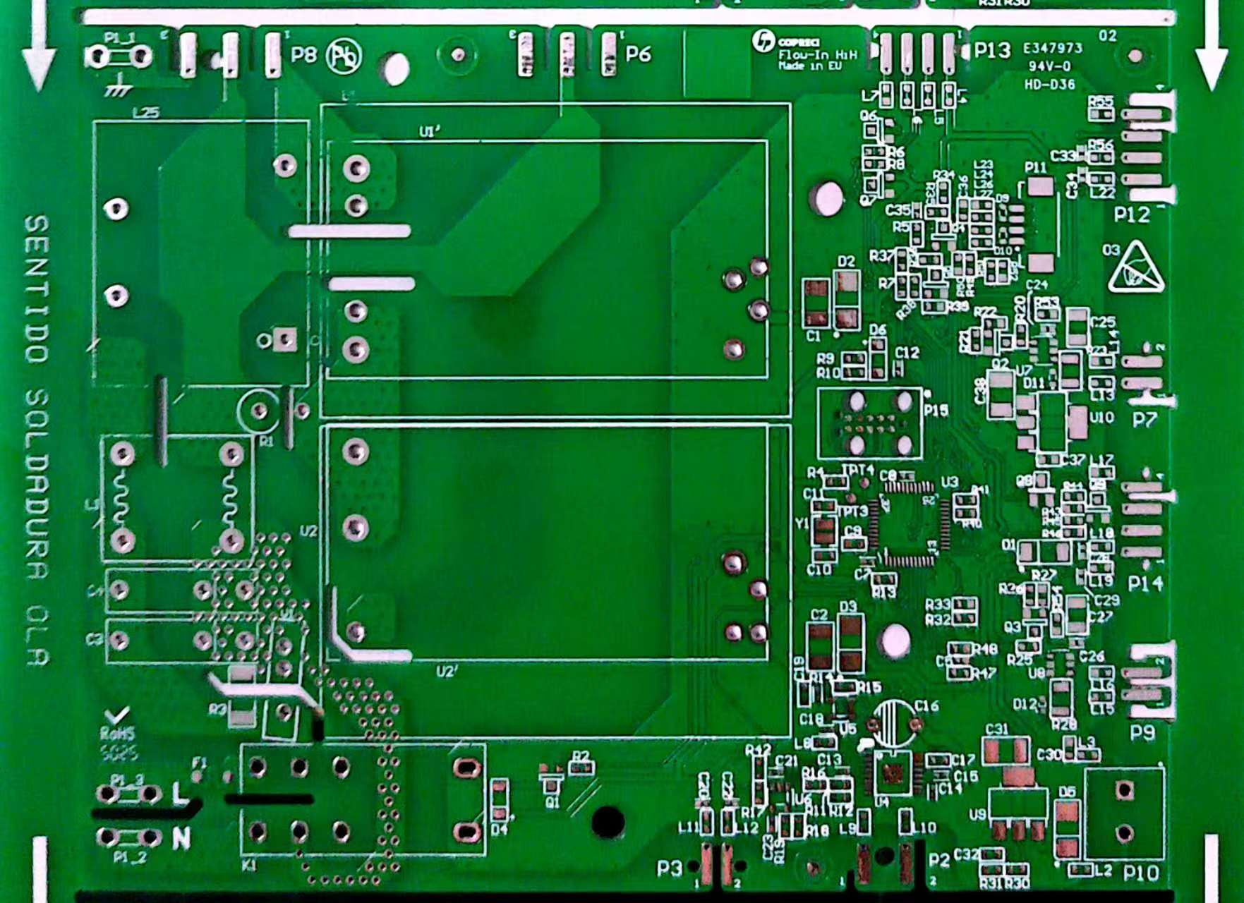
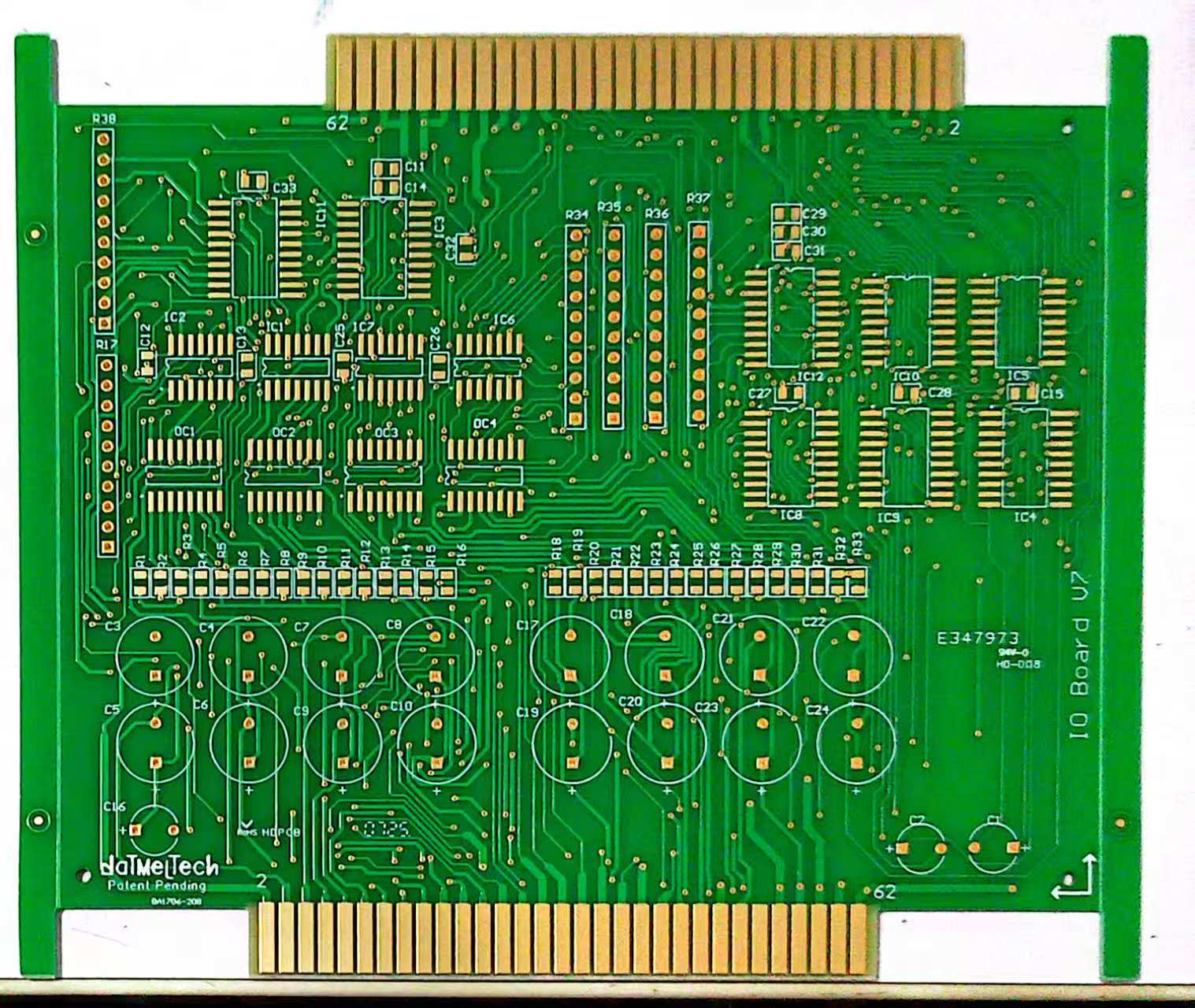
双面板应用场景
工业控制设备
电源模块
通信设备
汽车电子
医疗电子